-40%
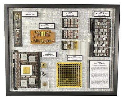
IBM Large Systems Technology - Pluggable Unit, SMS, SLT MST, HD-MCM, TCM
$ 739.2
- Description
- Size Guide
Description
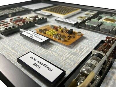
About this Artwork:This artwork is a collection of technology from IBM's large computing systems. The background image was created by photographing an actual IBM 3090 TCM chip using a microscope and special lighting.
Please note: this is the exact artwork you will receive.
IBM has been a leader in large systems technology for decades. Early on, these systems were called mainframes because the processor logic was held in the main frame of the system. In the late 1940s, IBM introduced pluggable unit vacuum tube technology. In the 1950s, it developed standardized boards to take advantage of transistor technology. In the 1960s, IBM began a long history of using multiple silicon chips connected on a ceramic surface. In the 1970s, this technology evolved into Multi-Chip Modules (MCMs) with ever increasing transistor density of the chips mounted on them. By the 1980s, these MCMs were so hot that they needed to be cooled with water. These MCMs were called Thermal Conduction Modules (TCMs).
For most of the 20th century, IBM had the most powerful single image computers (i.e., one operating system controlling all computing resources.) The following describes the technology of the various boards in this artwork.
1948 – The Pluggable Units:
The IBM Pluggable Unit was invented to meet the technology needs of the IBM 604 Electronic Calculating Punch. IBM anticipated the IBM 604 would be sold in the thousands. The challenges of building, testing, and maintaining these many electronic machines had never before been considered. IBM had only made 100 of the first electronic calculators in production. The Pluggable Unit had a vertical dimension rising off the flat mainboard. It provided greater circuit density and space savings. Each Unit was a simple circuit and could be tested independently of the 604 machine. If any component of the circuit was defective, the complete Unit could be quickly replaced to get the 604 operational, and then the Pluggable Unit could be repaired, and then reused. The time needed to manufacture and maintain the 604 was significantly reduced. When introduced, the 604 was the fastest calculator on the market.
1961 – The Standard Modular System (SMS):
SMS circuit boards were used in IBM computers in the 1950s and 60s until they were replaced by the System/360's Solid Logic Technology. SMS boards are 2.5 inches wide by 4.5 inches long. Double SMS boards were about 5 by 4.5 inches. SMS boards contained discrete (individual transistor, resistors, capacitors, etc.) components on one side. The board in this artwork is for an IBM 7030 Stretch supercomputer. This was IBM's first transistorized supercomputer and was the fastest in the world from 1961 to 1964. In addition, SMS boards were used in the IBM 7090 and the IBM 608. The price of this board was , which would be about 0 in today's dollars.
1964 – Solid Logic Technology (SLT):
In 1961, IBM had about 65% of the market for computers. However, IBM's existing computers were all incompatible. IBM needed a new approach to computing if it was going to gain, or at least hold onto its market share. IBM needed to step up its game. CEO Thomas Watson Jr. bet billion when IBM was only making .5 billion a year that the IBM System/360 was the answer. The introduction of the System/360 in 1964 was a major milestone in computer history. The top circuit board is part of an IBM System/360 processor. Each of the metal squares is a Solid Logic Technology circuit, which together provided the control, arithmetic, and logic functions of the computer. The board just below it has had the aluminum cans removed and exposes the SLT circuit. The SLT was the industry's first high-volume, automatic, microminiature production of semiconductor circuits. Mounted on 1/2-inch-square ceramic modules, the SLT circuits were denser, faster and required less power than the previous generation of transistor technology. The silver/gray traces on the surface connect the various components into a circuit. The tiny silver squares are transistors or diodes. The black areas are resistors. This technology was called hybrid chip technology because it mixed planar chip technology and discrete components in the same device. It is also called a Multi-Chip Module The third board was from an IBM System/360 model 67 mainframe computer. This board is "2nd generation" because, in addition to the Solid Logic Technology (SLT) Chips, a hybrid technology, it also includes flat pack logic chips, a pure planar technology. The SN2483A logic chips were made by Texas Instruments as a custom circuit for the System/360.
1970 – Monolithic System Technology (MST):
MST was developed for the IBM System/370, the next generation after the IBM System/360. Like the earlier Solid Logic Technology chips, the MST circuits were mounted on 1/2-inch-square ceramic modules. Whereas the SLT used individual transistor chips, MST used one or two multi-circuit integrated circuits to increase density, speed, and reliability. The board in this artwork is from an IBM System/370 Model 155.
1979 – High Density Multi-Chip Module (HD-MCM):
The HD-MCMs expanded on the MST concept by literally expanding the ceramic substrate. Most HD-MCMs used a one-inch square ceramic substrate and had more, larger, denser chips. Some of the faster/hotter chips were placed on two-inch ceramic substrates even though only a one-inch area was used for the chips. HD-MCMs were used in IBM’s 9370 and 4300 series systems. The HD-MCM board on the front is a processor logic board from an IBM 4361. The MCM chips to its right have had their covers removed to expose the chips. The top one has 4300 memory chips. The bottom two have 4300 processor logic chips on them.
1980 – Thermal Conduction Module (TCM):
The water-cooled IBM 3081 series introduced Thermal Conduction Module technology. The 3081 was the first processor to implement an Emitter Coupled Logic (ECL) bipolar circuit TCM – very fast, but very hot. The IBM 3090 Processor was also a water-cooled mainframe. Introduced in 1985, the 3090 contained four central processors and 128 MB of central storage. The MCM here has been removed from its TCM metal housing.
Six inches square, and 3.5 lbs, the 3090 TCM had room for up to 132 chips, each with 612 ECL circuits. Each ceramic block of the material had 20 - 22 differently wired layers. More than 470,000 holes provided paths for the vertical wiring allowing layer-to-layer communication. The chips were joined to the substrate through a total of nearly 18,000 contact points, using IBM’s unique chip-joining technology. All that circuitry generated 525 watts of heat, enough to destroy the chips. But the heat was drawn off through spring-loaded aluminum pistons (seen in the cutaway section) that pressed gently against each chip. In turn, the pistons were housed in a “hat” filled with helium, an excellent heat conductor. Chilled water flowing through a conduit attached to the hat whisked the heat away. One TCM alone (there were about nine in a 3090 computer) packed as much computing punch as a medium-size System/370 of only a decade before. In the 1980s, these TCMs would have had a value of about 0-350,000 each. Now, most TCMs have been destroyed for their gold. Check out the cutaway above that shows the inside of an IBM TCM with the MCM chips and pistons. This was the industry’s most advanced MCM.
Framing:
The artwork is framed in an 16"x20" black shadow box frame, with glass. All framing materials are acid free. A narrative about the artwork that includes the artist’s signature is placed on the back of the artwork.
Want to see more ChipScapes?
Click here to see more ChipScapes
TM
in my store on eBay
General Information:
These artworks are the creation of
ChipScapes
TM
artist Steve Emery.
ChipScapes
TM
are photographs taken of computer chips, boards, and other computer artifacts. They are sort of chip landscapes, or
ChipScapes
TM
for short. Most often a macro-lens or microscope is used with special lightning to achieve these unique artworks.
Intel, IBM, Fairchild, DEC, Signetics, Intersil, AMD, Zilog, Motorola, MOS, NEC, Texas Instruments, are some of the great chip making companies. Chips like the Intel 4004, MOS 6502, Zilog Z80, AMD 2901, IBM PowerPC and others have changed the way people work and play.
ChipScapes
TM
are dedicated to preserving and sharing these computing and communication technologies that changed the world.
ChipScapes
TM
artworks are fine collectible artworks.
ChipScapes
TM
come is a variety of shapes sizes and colors. Clusters of my artwork make for stunning displays! A
ChipScape
TM
would make a great gift for the nerd, geek, engineer, programmer, IT executive, or just that technology savvy person in your life.
More Questions?
For more information about ChipScapes
TM
, please check out my ChipScapes.com
website.
For more information about chip collecting as a hobby
,
please check out my
AntiqueTech.com
website.
